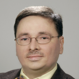
Hans-Jürgen Thees
Angestellt, Senior Principal Technology & Innovation, Infineon Technologies
Dresden, Deutschland
Werdegang
Berufserfahrung von Hans-Jürgen Thees
Bis heute 6 Jahre und 10 Monate, seit Sep. 2017
Senior Principal Technology & Innovation
Infineon TechnologiesResearch and development of next generation Si IGBT and SiC MOSFET technologies
4 Jahre und 7 Monate, Jan. 2016 - Juli 2020
Member of Industry Endorsement Board
IONS4SET Horizon2020 project
Appointment to the Industry Endorsement Board of the Horizon 2020 EU-Project "IONS4SET" which is researching on low-energy dissipation SET (Single Electron Transistor) quantum devices.
7 Jahre und 9 Monate, Dez. 2009 - Aug. 2017
Senior Member of Technical Staff, Technology & Integration, Microprocessors
GlobalfoundriesTechnology development FEOL 22nm FDSOI; Process integration FEOL 28nm/32nm PolySiON and HKMG technologies; Successfull technology qualification of 28nm performance node; Promotion to Senior Member of Technical Staff; Technology transfer 40nm FEOL for Japanese IDM, embedded DRAM, low power;
7 Monate, Mai 2009 - Nov. 2009
Quality and Integration Engineer, Organic TFT
Plastic Logic GmbH
Development of organic semiconductor technology and quality assurance policies
4 Jahre und 4 Monate, Dez. 2004 - März 2009
Technology team lead DRAM/eDRAM, Process Change Board Chair
Qimonda Dresden GmbH & Co. OHG
Technical management of interdisciplinary engineering group for Qimonda at Infineon Dresden 200mm plant, interface function to international DRAM fabcluster and to Infineon; 46nm buried wordline DRAM technology development
4 Jahre und 4 Monate, Aug. 2000 - Nov. 2004
Integration Module Engineer, DRAM/eDRAM
Infineon TechnologiesProcess integration of deep trench / shallow trench isolation modules, 110/170/200/240nm DRAM and eDRAM technologies
5 Jahre, Sep. 1995 - Aug. 2000
Development Engineer, Mixed-signal CMOS and EEPROM
ZMD AG
Development / Production of mixed-signal-CMOS-technologies (0.6/0.8µm), EEPROM Research projects with universities and institutes
Ausbildung von Hans-Jürgen Thees
10 Monate, Okt. 1994 - Juli 1995
Electrical Engineering
North Carolina State University, Raleigh, NC, USA
Research and thesis work on ultrathin nitrided gate oxides / 0.25µm technology
5 Jahre, Sep. 1990 - Aug. 1995
Electrical Engineering, Semiconductor Technology
Dresden University of Technology, Germany
Electrical Engineering, Semiconductor physics and technology, Sensors, Chip design, Material Science and Analysis
Sprachen
Deutsch
Muttersprache
Englisch
Fließend
